MEMS evolution: from Silicon to Polymers
By Fred Hussain
In the beginning…
In the 1970s, with the advancement in semiconductor microelectronics, researchers such as John Greenwood worked on wet anisotropic etching of bulk single crystal silicon to form 3D geometries, including diaphragms, beams, masses, grooves and holes at the µm scale. This led to the use of silicon and glass almost exclusively in microfabrication or MEMS. Silicon, a well understood electronic material, could then be sculpted into mechanical shapes with super elasticity, strength greater than steel and high stability. Many tiny devices could be produced in parallel on a single wafer and the processes could be precisely controlled, scaled up and made repeatable. This resulted in new classes of silicon and glass devices, including pressure sensors, accelerometers and gyroscopes that were quickly adopted by the automotive industry, as well as the emergence of micro-valves, micro-pumps and gas/bio sensors, applicable in life science and other industrial applications.
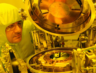
In 1982, Kurt E Petersen, known as the father of MEMS, wrote an important paper, “Silicon as a Mechanical Material”, which was the catalyst of much MEMS research, mainly in the US universities and institutes, including, MIT, Sandia, UC Berkeley and Stanford. In the UK, there were only a handful universities, including Southampton, who developed their microelectronics cleanrooms to enable MEMS research.
Commercial interests
In the 1980s, companies such as Epson, HP and Canon started producing inkjet printers utilizing MEMS for accurate actuation and print nozzle manufacture. IC giants, such as Motorola, Bosch and Analog Devices also made many MEMS sensors. Kurt Petersen founded Novasensor, making pressure and acceleration sensors using silicon and glass. The first accurate silicon gyroscope was developed by BAE SYSTEMS in Bristol at the same time. In the early 2000s, it was then the telecom companies, such as JDS Uniphase and Nortel Networks, who poured millions into MEMS/MOMS(micro-opto-mechanical systems) making micro-optical benches, mirrors, switches etc. Finally, in the late 2000s, the mobile phone industry pushed MEMS to another level of miniaturisation, performance, power requirement, cost and volume. Packaging was also being miniaturised with through-wafer-vias (Corning and Schott) and 3D integration.
Why polymers?
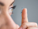
The current decade has seen the MEMS market increase in size with exciting new applications in the life sciences and bio-medical industries, where longer micro-channels, increased sample volumes and chip size are cost-prohibitive for silicon and glass. Also, transparent micro-channels with vertical and deep wall profiles are not easily achievable in glass. Photosensitive glass, such as FOTURAN, made a promising start, but was discontinued due to strong competition from soft lithography, laser machining techniques (e.g. Femtoprint) and of course polymers. Other applications such as tactile sensing and flexible displays required flexible substrates and bio-sensors needed certain polymer chemistries to attach to. Polymers were the natural answer and even though first used in the 1980s, they are only now gaining significant popularity.
Polymers have the following advantages:
- Material properties – many polymers can withstand greater mechanical strain than silicon and are not as brittle. They can also be engineered to have lower thermal expansion. In addition, they can made be optically transparent with low fluorescence, inert to their environment and biocompatible, essential for many microfluidic devices.
- Wide process toolbox – the silicon/glass micromachining toolbox is relatively limited compared to polymers. Polymers can be directly photo-patterned and etched, micro-moulded, dry (RIE) or chemically etched, laser ablated, created by stereo lithography, 3D or screen printed, hot-embossed or imprinted/stamped and bonded at the wafer scale by plasma, thermal fusion, or using surface modification e.g. using silanes and epoxy
- Low cost – for the same area, silicon/glass substrates typically cost 10-100 times more than an equivalent polymer. Furthermore, many fabrication techniques employing polymers can be performed in low-cost labs rather than cleanrooms.
Challenges?
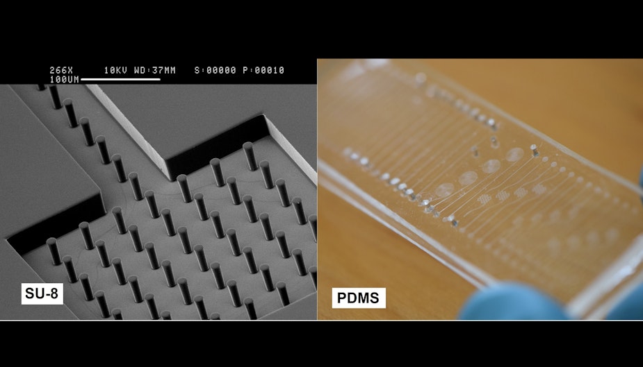
As with every material, there are still some challenges with the use of polymers, including: temperature stability, performance over time, chemical compatibility, optical properties, electrical charging and low dielectric breakdown. PDMS is a great material for many lab-on-chip applications, replacing glass. However, its drawbacks include removal of trace organic compounds from solutions, inherent hydrophobicity, gas and water permeability and higher fluorescence than glass. Thin film PDMS can be difficult to work with, particularly at commercial scale. Bonding of COC, PMMA or other plastics to glass can be difficult due to thermal mismatch. And hot embossed polymers can limit life-time of fragile silicon/glass masters.
In the future
Silicon and glass are unlikely to become extinct, but they could soon be replaced by polymer alternatives in many applications. New classes of liquid and dry film polymers are being developed and taken to commercialisation, i.e. mixed with conductive, shape memory, photosensitive, piezoelectric, plastic magnet, electroactive, OSTE and polypyrrole elements. Such polymers or smart materials are opening new and exciting opportunities, particularly in the life science and bio-medical fields, e.g. in artificial muscle actuators, tools for invasive robotic microsurgery, actuators to stimulate tissue and bone growth and a whole host of bio-sensors, lab-on-chip and µTAS systems. The next few decades could see amazing advances in MEMS technologies using polymers.

Related Articles