How to develop microfluidics for commercial products
By Fred Hussain
Whilst microfluidic devices have huge potential, most fail to progress beyond research use, let alone reach mass consumer markets similar to products in the microelectronics industry. But developers are increasingly using cycles of (1) optimised designs, (2) apt manufacturing, and (3) robust testing to create highly integrated and compact devices with exciting functionality for widespread application.
Microfluidic systems have reached a staggering level of maturity, with a multitude of ingenious devices and individual components able to match the performance of traditional lab-based counterparts. Significant opportunities remain to translate microfluidic systems from research use into products. In this blog, we distil some of the experiences gained during the development of a microfluidic device for Cellular Highways.
In this blog, we cover:
– How microfluidic modelling can accelerate development
– What materials and techniques are available for prototype and volume production?
– What can be learnt about testing and transfer to volume manufacture?
How can CFD packages accelerate development?
The development of a novel microfluidic device begins with the design of a prototype device. Traditionally, the main features of the design – such as channel geometry, material properties, applied pressure/flow, mixing and hydrodynamic effects – were derived from simplified calculations, based on experience and intuition. Whilst simple, this approach risks ignoring important or hard-to-grasp effects and then requires numerous costly fabrication–test cycles.
Now, computational fluid dynamics (CFD) packages such ANSYS and COMSOL can be used comprehensively to reduce costs and iteration times dramatically, allowing designs to be trialled without going to the lab. A good understanding of the modelling attributes will facilitate the rapid transfer of an idea for a microfluidic system to the prototype stage.
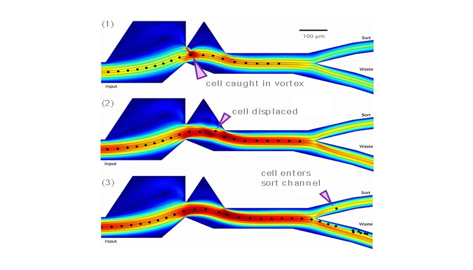
Modelling was key to the development of a vortex-actuated cell sorter (VACs) for Cellular Highways. In this case, the expansion and collapse of a thermal vapour bubble were modelled using a “moving wall technique” and moving the boundary locally by a realistic amount simulated the bubble. As a result of this novel modelling approach, between 20 to 30 vortex concepts were trialled, and the final design worked in the first real prototype PDMS device.
Materials and techniques for prototype and volume production
A design that works on paper (or in simulations) will only become a product if it can be fabricated and ultimately scaled to volume manufacture at an appropriate price point. Different fabrication techniques are available at different stages of the development, whilst material selection is also an important consideration. Below are a few examples.
(i) Prototype
PDMS is a versatile, low cost, transparent material ideally suited to prototyping and low volume applications and can be easily bonded to glass. Working with PDMS does not require a costly cleanroom. However, due to potential contamination of microfabrication equipment, many MEMS foundries will avoid it and it can have some adverse effects on cells.
Other techniques suitable for prototyping include 3D printing. Dolomite Microfluidics’ 3D fluidics printer is great for rapid design iterations but produces rounded cross-sectional shape due to layers built up from extruded plastic.
Projection micro-stereolithography uses mirrors and UV light to polymerise planes of resin to create 3D features, but most resins are non-biocompatible. Using femtosecond lasers (e.g. Femtoprint) plus etching of glass can also be used to produce intricate 3D structures for prototypes, although this can be a costly and slow (serial) process for volume production.
(ii) High volume
Most high-volume and perhaps low-complexity and low-cost disposable applications tend to use thermoplastics. These materials (e.g. COC, PMMA, PS, PC, PEGDA, etc.) can be moulded/re-moulded upon reaching their glass transition temperature (Tg), typically using hot embossing, injection moulding (high set-up costs) or even direct (micro) machining techniques. Normally, the same polymer with the inlets/outlets is thermo-compression bonded to seal or cap the channels, but care is needed in selecting the pressure, temperature and timing profile, in order to not collapse the sub-surface microchannels. Reel-to-reel processing, although costly to set up, can allow larger volumes and therefore lower costs.
(iii) Mid volume
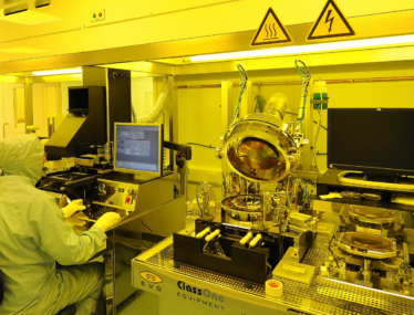
Microfluidics had its roots in microfabrication or MEMS (micro-electro-mechanical systems) mainly through early digital printing and gas chromatography in the mid-1970s. MEMS fabrication requires costly cleanrooms and specialised equipment, so many people reject it out of hand. But MEMS-based chips are perfectly acceptable for small and high-volume applications, as demonstrated by the devices within mobile phones and cars.
For microfluidic applications, the chip size is typically in the centimetre range, hence the mid volume-cost category. Silicon supports several functions, including integrated electronics, sensing and actuation. If transparency is required, then a glass layer can easily be (anodically) bonded to silicon, whilst 3D sculpting of silicon, glass or both materials is relatively straightforward. Important steps such as dicing of final chips and making electrical & fluidic contacts, as well as good metrology cannot be ignored.
An alternative to MEMS in the mid volume-cost category is the use of ceramics, typically aluminium oxide or low-temperature co-fired ceramics (LTCC). They have a history in military, space and printing applications. Advantages of LTCC include integration with sensors/electronics, screen printed layers and easy machining via lasers, albeit feature sizes are generally coarser than for silicon or glass.
During the development of a vortex-actuated cell sorting device for Cellular Highways, many cleanroom processes were investigated, including the direct making of SU8 and Ordyl microchannels, but these auto-fluoresced. COC plastic was then successfully embossed with micron-sized features using SU8 on silicon masters, but the embossed part poorly bonded to glass due to a thermal expansion mismatch. COC was then replaced by PDMS which was plasma-bonded to glass and helped optimise designs quickly. As discussed earlier, MEMS foundries were reluctant to work with PDMS and therefore the final product evolved towards the use of glass for the microchannels, bonded to silicon.
What can be learnt about testing?
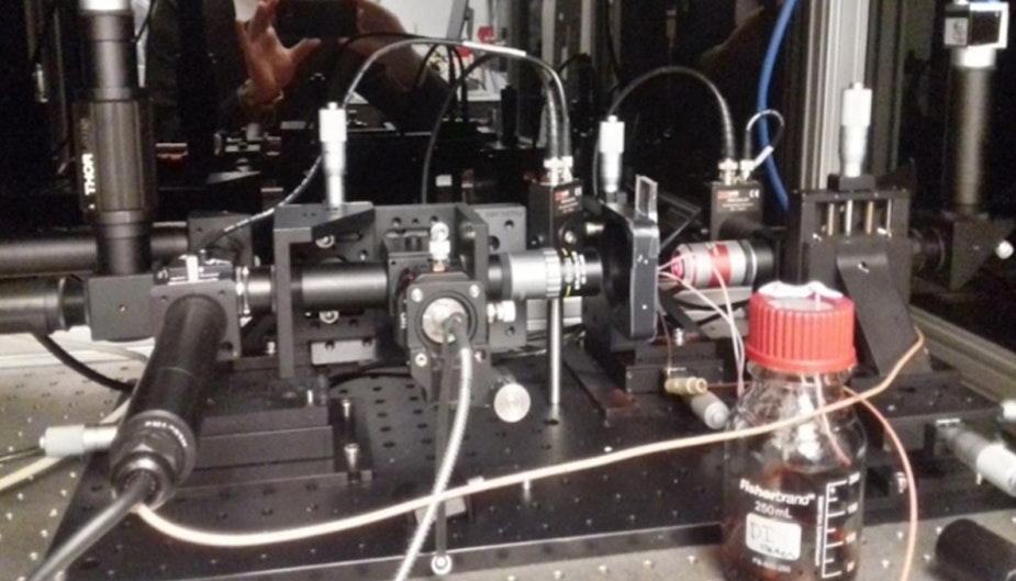
During device development and verification, it can be immensely valuable to replicate standard workflows to allow benchmarking of performance. In addition, dividing more complex workflows into component steps can simplify testing. For example, a PCR-based diagnostic device could be assessed in terms of sample lysis, nucleic acid extraction, and thermocycling.
Device testing and design iterations require close cooperation between biology and engineering teams, plus the need for appropriate facility and equipment. For devices involving manipulation of particles (e.g. magnetic microspheres) or simple biochemical assays, basic optic and lab equipment will be sufficient. Where testing involves cells or clinical samples, however, appropriate biological safety containment laboratories staffed by qualified staff are a must.
Characterising physical and chemical effects, including surface roughness, capillary forces, and chemical interactions between materials, is important because these become more significant at the microscale. This can often result in complications during on-chip experiments that would not be expected with traditional lab equipment. Similarly, air bubbles, which can create stress to cells and even lead to cytotoxicity can be a serious obstacle to a successful long-term operation of microfluidic systems, and bubble traps may need to be incorporated.
Connecting the microfluidic device to the macroscopic world, which is necessary for the development of an eventual product, can present its own unique technical challenges. Reliable interfaces to connect the channels and tubing for the transport of liquids are required, as device performance might be impaired by leakage, particulates or bonding agents. Access ports also need attention; laser ablation creates melt-back, direct drilling or coring is slow and can suffer from debris. Deep RIE or wet etching is commonly used on silicon and glass.
Whilst the above is not an exhaustive list of considerations that crop up during testing, not considering them may result in costly design iterations and/or worse jeopardize the functionality of the whole system.
Transfer to volume manufacture
Once the prototype product is established, the next step is to take the detailed SOPs and specifications to ISO-accredited foundries that can assess volume manufacturability. However, if the required volume (wafer count) is too low (or too high), then your emails/calls may be ignored. The alternative is to build your own capital-intensive laboratory or cleanroom, but this is probably not a viable course of action for most start-ups. There are of course many other hurdles to overcome, such as quality accreditation, medical trials, FDA approval and of course running the business, all of which can feed into the microfluidic development cycle.

In conclusion
Microfluidics covers a wide range of possible products and applications. Microfluidic developers can now deliver devices capable of mass application and commercialisation. Success relies on the understanding and utilisation of (1) optimised design modelling, (2) appropriate material choice and process selection, and (3) running tests using suitable equipment and laboratories – and learning rapidly from previous iterations in the microfluidic development cycle.
How we help our clients | Healthcare | Industrial | Consumer | Healthcare Blogs | Industrial Blogs | Consumer Blogs | Healthcare Case Studies | Industrial Case Studies | Consumer Case Studies