Multi-Project Wafer (MPW) services were first introduced in the 1980s (by MOSIS) to share space on silicon wafers and counteract very high Integrated Circuit (IC) development costs. For ICs, this was relatively straightforward, given the highly standardised fabrication processes and excellent function libraries, which allow developers to efficiently transfer sub-units between designs. Following on from MPW prototyping, scale-up to higher volumes was relatively easy.
Now MEMS foundries also offer MPW services, even though microfabrication covers a much wider range of processes and materials, including bulk or surface micromachining, silicon-on-insulator (SOI), wafer bonding integrated with electronics/photonics/piezoelectrics/bio-elements.
MPWs can be a low-cost and accessible way of making your first MEMS chip, but what do you need to know before choosing this route? In this blog, we discuss the pros and cons, alongside examples of three TTP-internal MPW projects, ranging from more conventional bulk microfabrication to lesser-known polymer and plastic-related processes.
Key points in this blog:
- Examples of MPW MEMS projects
- Design rules and their importance
- Scale-up considerations
- Scheduling and costs involved
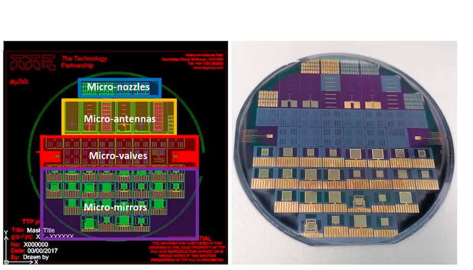
Multi-Project Wafer project examplesBulk microfabrication using SOI wafers
Bulk microfabrication using SOI wafers
Most MEMS foundries offer materials and processes such as surface or bulk microfabrication using silicon and glass. SOI wafers are a common starting point and with well-established processes can offer complex, high aspect-ratio and accurately layered devices – a core process offered by many MEMS labs and foundries.
In this example, we used SOI wafers to manufacture four different “micro” devices: micro-mirrors, micro-antennas, micro-nozzles and micro-valves. The project used the same mask-set, process and materials for all the devices, thereby saving approximately 25 percent on the overall project cost and timescale. A key advantage was the inclusion of multiple designs on the same wafer, with 10mm x 10mm sized chips made using low-risk processes available at most MEMS foundries.
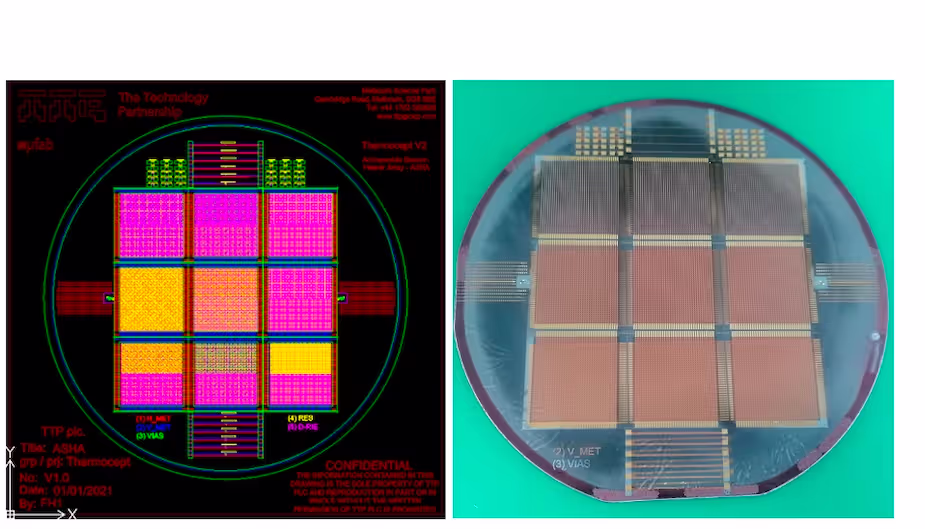
Silicon-polymer process
Polymers such as PDMS and SU8 are commonly used for microfluidic device prototyping, as discussed in my previous blog. They show a wide variety of desirable properties, support both quick prototyping, low-cost and a rich process toolbox.
This project involved the making of polymer layers containing thermal elements for two applications, heated pixel and thermal sensor arrays. Devices consisted of arrays of resistors at 0.5mm pitch, horizontal and vertical metal tracks separated by SU8 polymer layers and via holes to connect each layer electrically. There were nine designs, each with a die size of 22mm x 22mm. The range of devices and layout allowed us to address the needs of multiple stakeholders on a single chip, dramatically reducing development cost.
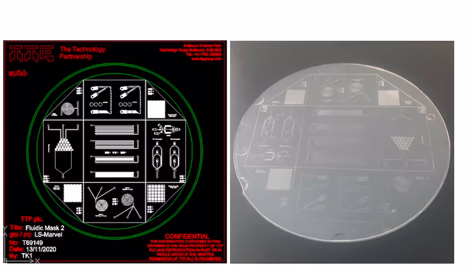
Hot embossing and sealing using low-cost polymers
Hot embossing allows rapid polymer processing and is suitable for large area, high volume and low-cost devices compared to silicon and glass. The process consists of making electroplated metal masters, then hot embossing on to plastics (COC, PMMA, PC, PS etc.) followed by capping using heat, chemicals or pressure-sensitive adhesives. In this project, we successfully demonstrated all the above steps using 28µm deep masters (later 50 µm and 100 µm). We offered the technology to different internal clients requiring microfluidic demonstrators and standardised building-blocks, thereby reducing development costs by 90%.
Design rules
Foundries tend to select MPW services based on their core expertise and processes. The process steps and materials are then ‘frozen’ alongside a good set of design rules and element libraries. This is relatively easy in the IC industry but can get complex in the more “3D” world of MEMS with many variables and lack of standardisation.
An inflexible and complex set of design rules can create higher barriers to MPW entry. Process uniformity is another potential issue to deal with. For example, in the D-RIE process, variations in the mask pattern density can produce etch non-uniformities and such knowledge, as well as the adding of dummy structures to improve the pattern density, can really help. Top MEMS foundries and their designers are aware of all these issues and have established, documented (SOPs) and qualified (repeatable and reliable) processes to minimise them. Alternatively, the specification window is widened to account for such process variations and loss of yield.
Scale-up
MPWs using low risk materials and high-yield processes make the subsequent scale-up more straightforward. However, plastics and polymers are less commonly offered for MPWs due to the large variety of materials, large die sizes and geometry variations across all the applications.
Wafer testing can represent 25–50 percent of the overall manufacturing cost due to the multi-physics nature of MEMS chips and so may be dropped by some MPW providers. So, some foundries deliver unpackaged and untested prototypes, but at additional cost some test along with dicing, encapsulation and wire bonding can be included. Packaging requirements are generally more bespoke and depend on the specific chip and application, so they are either dealt with at wafer scale (anodic bonding) or individually, say through 3D printing for example.
Scheduling and costs
To make MPWs viable, MEMS foundries typically wait until most of the wafer area is sold before commencing work. Some offer up to 6 wafer runs per year depending on popularity and market demand. If you miss the deadline or there is insufficient demand, then you may have to wait until the next available run.
MPW costs are proportional to the die number, total area used, complexity and masking steps, typically in £/sq-cm or £/chip. As an example, a European university-linked foundry can charge 1,000 – 1,500 Euros for approximately 100 chips to students, and 4,000 – 6,000 Euros for industrial clients.
Summary
Sharing space on a wafer through MPWs could be the most effective way of making your first MEMS device, particularly if you have no cleanroom access, as discussed in my previous blog. If the design is submitted on time and the schedule works well, then you could achieve several iterations and reach scale-up volume within a year, or so.
However, lack of MEMS standardisation, wide range of processes and materials, lack of testing due to the multi-physics nature, and design-related process variations can all affect the yields. This in-turn can create differences between the different MPW providers. Europractice is a good place to find foundries with core strengths that they then offer as MPWs, thereby reducing any overlap or competition, whilst maintaining certain quality standards. So, aligning your process steps and materials with one of these foundries, through MPWs could enable your MEMS idea to soon become a scaled-up product.
References
01. The Quantum Age: technological opportunities, Government Office for Science, 2016.
02. Strategic Intent, UK National Quantum Technologies Programme
03. Quantum gold rush: the private funding pouring into quantum start-ups, Nature, 2019.
04. Commercialising Quantum Technologies: germinator projects round 1.
05. National Quantum Computing Centre Commercialising quantum computers, Economist, 2020.
06. Commercialising quantum computers, Economist, 2020.
08. Integrated quantum systems, M Squared.
09. A cryogenic CMOS chip for generating control signals for multiple qubits, Nature Electronics, 2021.