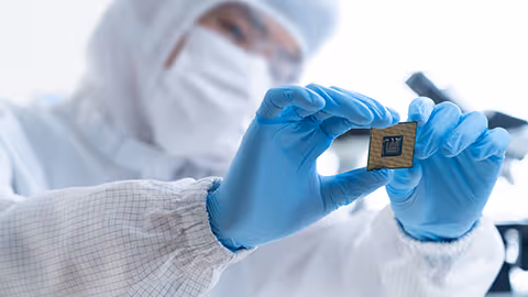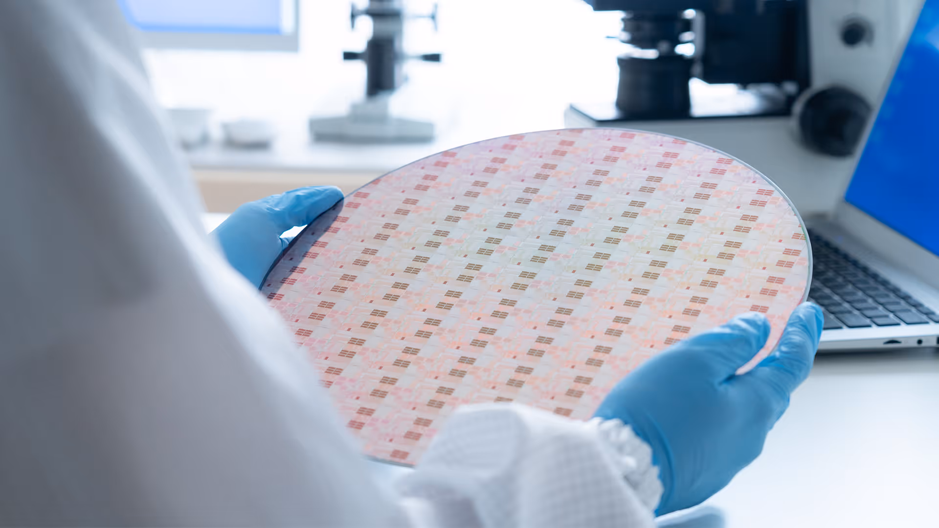
As chip feature sizes move to 10 nm and below, even sub-10 nm particles can materially reduce manufacturing yield. Clearing these ultra-fine contaminants from photomasks and wafer surfaces is increasingly difficult because modern structures are complex, surfaces are highly damage sensitive, and particles at this scale can be effectively invisible to conventional inspection and handling approaches.
This whitepaper reviews the fundamental mechanisms that govern wafer and photomask cleaning, then looks ahead to emerging techniques and process modalities designed to improve removal performance while maintaining device safety. The focus is on raising removal efficiency and strengthening process reliability as nodes continue to scale.