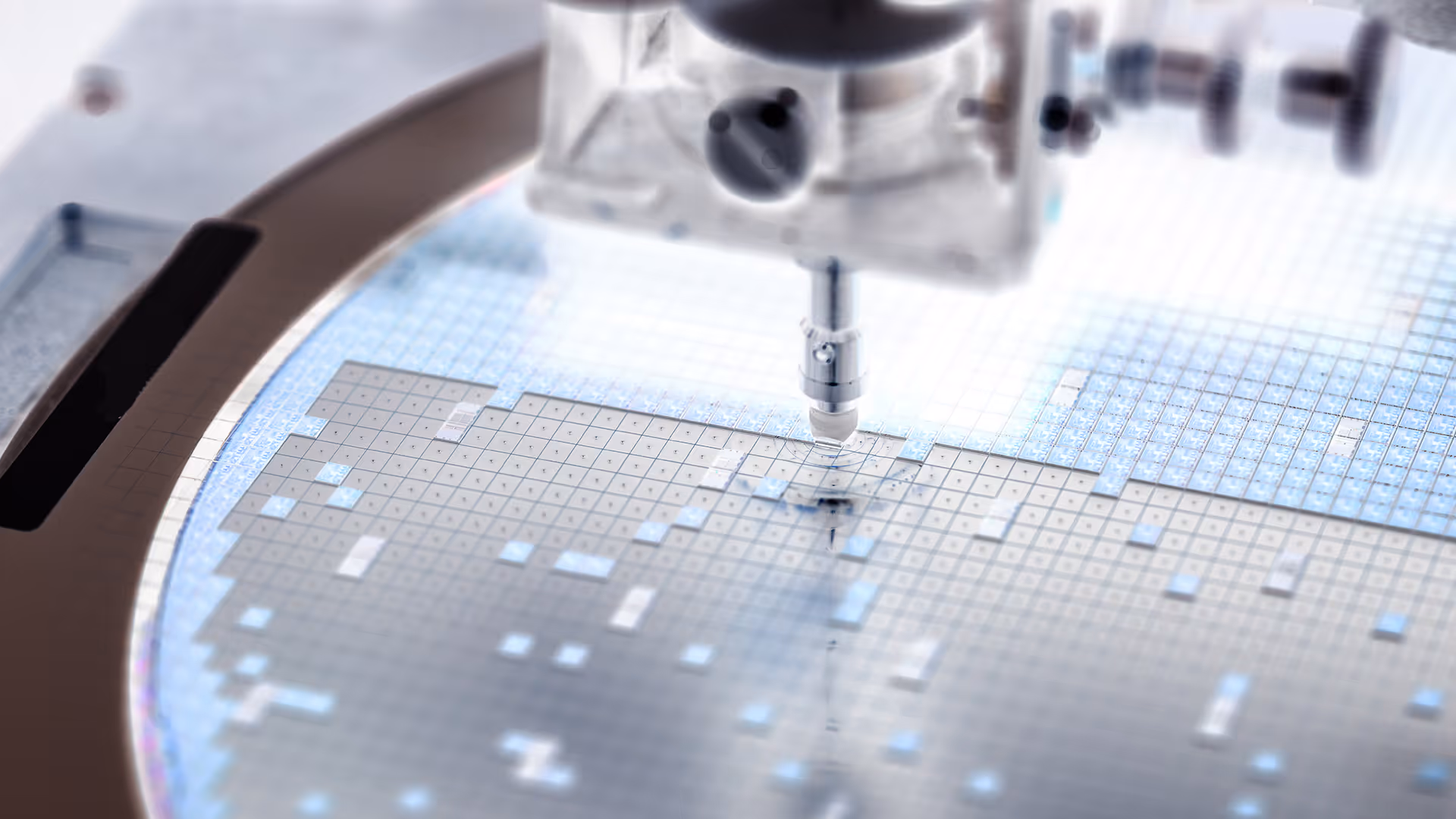
As chip feature sizes shrink below 10 nm, plasma assisted etching and thin film deposition must deliver ever tighter control, uniformity, and repeatability. In parallel, advances in computational resources mean computer simulations are increasingly crucial for developing plasma reactors, enabling faster exploration of process windows and reducing costly experimental iteration.
This whitepaper outlines the plasma properties and processes that matter most for etching and depositing atomic layers. We then present numerical simulations that elucidate, control, and optimise ion energy, one of the key process parameters for achieving nanoscale precision.